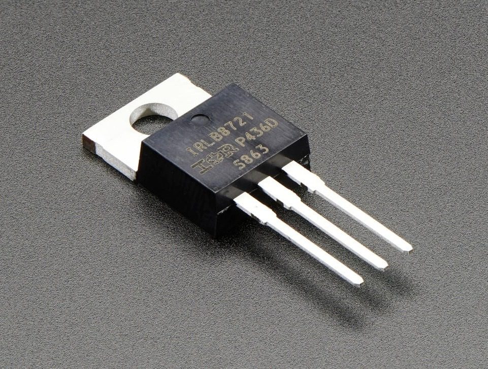
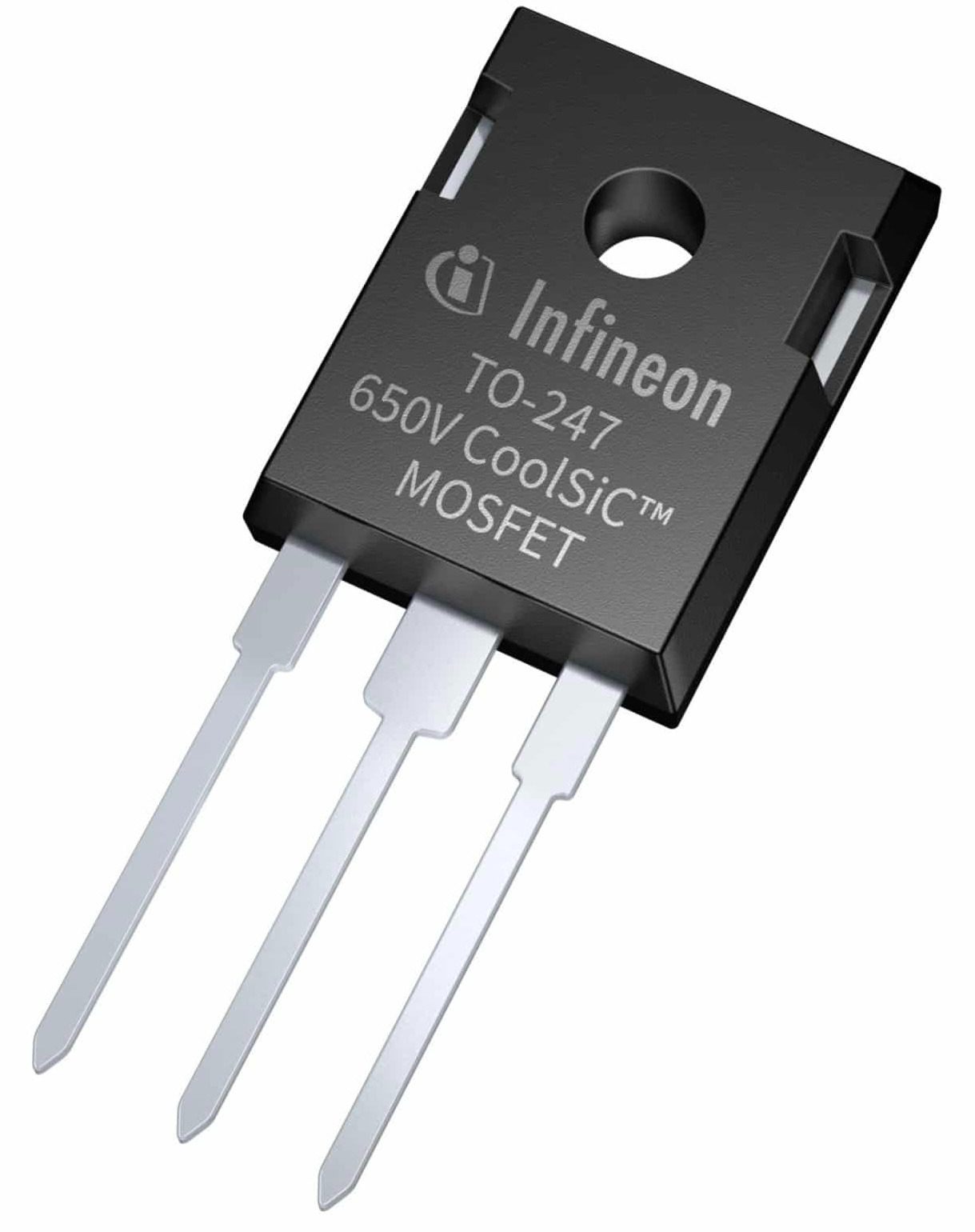
The history of modern microchips is incomplete without the name Robert Bower—an American physicist, engineer, and inventor who was at the forefront of revolutionary technologies in the semiconductor industry. He created the self-aligned-gate ion-implanted MOSFET, the technology that became the foundation for most integrated circuits, without which modern electronics would be unimaginable. His work transformed the theoretical developments of his predecessors into a practical breakthrough, and his name is forever etched in scientific history alongside titans like Kilby and Noyce. Bower was not only an inventor but also a teacher, a scientist, and the author of over 80 publications and 28 patents. More at i-los-angeles.
Biography
Robert W. Bower was born in 1936 in Santa Monica, California. He came of age as the world was just beginning to discover the possibilities of electronics. After high school, he joined the U.S. Air Force, where he served from 1954 to 1958. It was there that he first developed a serious interest in technical systems, a passion that would define his future path.
After his service, Bower enrolled at the University of California, Berkeley, where he earned a bachelor’s degree in physics in 1962 while working at the Lawrence Radiation Laboratory. The very next year, he obtained a master’s degree in electrical engineering from the California Institute of Technology (Caltech), and in 1973, he completed his Ph.D. in applied physics.
His career began at Hughes Research Laboratories in Malibu—one of the leading research centers in the U.S.—where he made his most important discovery. Later, Bower dedicated over 14 years to teaching at the University of California, Davis, where he became a professor emeritus and a mentor to a new generation of engineers.

A Revolution in Electronics
In the latter half of the 1960s, the electronics world was searching for a solution to shrink microchips and improve their precision. The principle of the transistor, first proposed by Lilienfeld in the 1920s, remained unrealized due to a lack of the necessary manufacturing technologies. Following the discoveries by Kilby and Noyce, who created the integrated circuit, and the research by Hofstein and Heiman, who described the MOSFET principle, a key problem remained: manufacturing precision.
In 1965, it was Robert Bower who solved this problem. He invented the self-aligned-gate ion-implanted MOSFET, a transistor that allowed for the creation of more compact, faster, and more energy-efficient microchips. His patent was officially registered in 1969. This invention became the foundation of the modern electronic age—powering everything from personal computers to smartphones and satellite systems.
Like many scientific breakthroughs, Bower’s discovery was accompanied by patent conflicts. Engineers Kerwin, Klein, and Sarace claimed they were the first to create the self-aligned gate transistor. However, back in 1966, Bower and his colleague Hans Dill had already presented the first scientific paper on this invention at the International Electron Device Meeting in Washington. After legal proceedings, it was established that Bower was the first to implement the principle of using the gate as a mask to form the source and drain regions through ion implantation. His patent became foundational for the entire industry. Bower’s invention not only solved a technical problem but also opened a new era in microprocessor manufacturing. The court recognized that the majority of transistors are manufactured using the ion implantation method described in his patent.

Publications and Research
Robert Bower left behind a powerful scientific legacy. He published over 80 scientific articles and journal papers, wrote three chapters in specialized books, and authored more than 28 patents.
His research covered topics from microelectronics to high-density three-dimensional structures. Notably, in the 1990s and 2000s, he worked with the company Integrate Vertical Modules, where he researched 3D technologies in the manufacturing of semiconductor devices.
His patents include:
- Aligned Wafer Bonding (U.S. 5,226,118, 1993) — a technology for bonding silicon wafers;
- Digital Pressure Switch Formed by Aligned Wafer Bonding (U.S. 5,294,760, 1994);
- Nitrogen Based Low Temperature Direct Bonding (U.S. 5,503,704, 1996);
- Transposed Split of Ion Cut Materials (U.S. 6,346,458, 2002).

Awards and Honors
Throughout his distinguished career, Dr. Robert W. Bower received numerous prestigious honors that recognized his significant contributions to the advancement of physics and semiconductor engineering. In 1986, he was elected a Fellow of the Institute of Electrical and Electronics Engineers (IEEE)—one of the most respected professional organizations in the world. He received this honor “for the invention of the self-aligned-gate ion-implanted MOSFET and for pioneering the application of ion implantation technology in the manufacturing of integrated circuits.”
His scientific achievements were repeatedly recognized at an international level. In 1997, Robert Bower was inducted into the National Inventors Hall of Fame in the U.S. for creating the MOSFET transistor that revolutionized semiconductor manufacturing. That same year, the U.S. Department of Commerce honored him with the Ronald H. Brown American Innovator Award, which is given for outstanding technological innovations that have a significant impact on American industry.
In 1999, Dr. Bower was elected a member of the U.S. National Academy of Engineering—one of the highest professional distinctions an engineer can receive. This election was a recognition of his lifelong contributions to the development of the semiconductor industry.
In 2001, he received two prestigious awards: the Alexander von Humboldt Award from the German foundation of the same name, which is a lifetime honor for world-class scientific achievements, and the Distinguished Alumni Award from the California Institute of Technology—the highest honor this renowned university bestows upon its graduates.
Two years later, Bower was presented with the Distinguished Senior Fellow Award from the physics department at Queen’s University Belfast. This award is given to scientists who have achieved international recognition in their research fields.
Even early in his career, Bower established himself as a world-class researcher. His paper, “Insulated Gate Field Effect Transistors Fabricated Using the Gate as Source-Drain Mask,” presented at the 1966 International Electron Device Meeting, was recognized as the most significant scientific report of the event. This work marked the beginning of a new era in the history of semiconductor technology.
After retiring, Bower continued to consult for research centers and write papers on the future of microelectronics. His research in 3D integration and nanoscale structures became the basis for developing technologies used in artificial intelligence, mobile devices, and quantum computing. He died on January 27, 2024, on the island of Maui, Hawaii, at the age of 87.
Robert Bower’s legacy is not just about technical inventions; it’s also a philosophy of limitless possibilities. His story is a reminder that even the most complex discoveries begin with a simple question: “What if?” Without his transistor, the world would have neither modern processors, nor smartphones, nor the billions of devices that manage daily life. Robert Bower proved that true engineering is the art of combining science, intuition, and a human passion for improvement.

